A while back I noticed a photomicrograph of a CDP1802 chip and it appeared that the goal was to produce a simulation like they had done for the 6502. I checked back on occasion but no progress seems to have been made. At least nothing is mentioned on those web pages. So since I once had some courses on VLSI design and have illusions that I know something about it, this page takes a look at bits and pieces.
The MOSIS service is still around so if someone was really motivated they could do a full layout and move the 1802 to a more modern process. It would be a lot more expensive than picking up an old 1802 off of ebay.
This covers the data path on the right half of the chip starting (more or less) from the top and working down.
The most obvious feature of the layout is the 16X16 bit address register file. Zooming in one cell of this looks like:
After staring at this for a bit I dug out my old VLSI design textbook and looked up the part on static memory. After a while, it was obvious that the standard six transistor SRAM cell shown there is identical to the design used here. (I have annotated the image with the identifiers used on that wiki page.) A pair of cross coupled inverters and two N channel transmission gates for control. The transmission gates are the N transistors on the inside while the outside ones along with the P FETs form the inverters. The bit lines run vertically while the word line is horizontal. The word line isn't as obvious because it is not a straight through metal run. Because this process used only a single metal layer it has to use poly-silicon to cross the bit lines.
This basic cell and its mirror image are repeated 256 times. It looks like the upper and lower bytes are alternated across the array. This simplifies the wiring to the multiplexer needed to output the address on the pins just above.
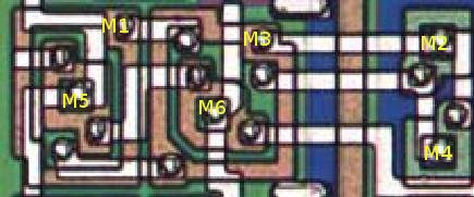
Just above the register file is another structure:
Inputs from two mirror image columns of the register array come in at the lower corners while the output to the pin is on the upper left. (in poly-silicon) There are only two signal lines that traverse the cell and they each connect to one half of this cell. So it initially appears that this is just a one of two mux.
Except that it is more complicated than required for a mux. The textbook transmission gate mux uses all of four transistors. There are also no obvious simple gates visible except for some inverters.
One of the odder features of this is that there are four transistors that have their sources isolated from the diffusion. They look like a transistor inside a transistor except that the outer transistor has its gate connected to the source so it is always off.
As an exercise I decided to dust off my long forgotten experience with the VLSI layout program Magic I used this in a graduate course more than a decade ago but it is still around.
As I was remembering things I realized I had a problem and that it might have something to do with an odd feature of the chip image. As is pointed out on the 1802 wiki, the n diffusion appears in the picture with a green color while the p appears as blue. In the space between the two regions in this section there are alternating bands of blue and green. This does make sense once you understand a few details.
The usual way of making a N channel FET is to start with a lightly doped P region (usually denoted as p-). Depending on the process this might be a well diffused into the starting n- silicon or it might be the base p- silicon. The first step is to lay down the poly-silicon traces that will be used for the gates. (And sometimes as signal lines.) The next step is to put down a heavily doped N diffusion (n+) across the poly-silicon. This results in what is called a self aligned gate. The poly-silicon line prevents the n diffusion dopant from altering the material under it, which creates the device channel. Then contacts are created between metal and the n+ region. In magic it looks like:

While searching for something else, I stumbled onto an old paper about a CMOS CCD that has a few more details on the C2L process. It includes this figure showing better details of the structure:

It shows it as being an n-well process with a guard band of poly-silicon around it. On the n-well side of the guard band is a ring of n+ diffusion while a p+ ring is on the other side.
I also found a paper discussing the use of the C2L layout for devices that might be used in the Large Hadron Collider. It references the 1977 RCA papers.
This isn't quite how it is displayed by Magic but it isn't getting along with xwd (X window dump). The vertical red bar is poly silicon, blue is metal1, green is n diffusion, and the darker boxes are the metal to diffusion contacts.
The key thing to remember is that operation of the FET depends on the gate to substrate voltage and not gate to source. In a discrete MOSFET the substrate is connected to the source. Here the device operation is symmetric.
As luck would have it I have a gif image of a chip I layed out long ago. It is just a basic 8X8 multiplier in a 2mmX2mm Tinychip frame:

If memory serves this used Booth recoding to reduce the eight partial products to four. The results of that are fed to two layers of carry save adders. (The carry is fed to the next stage rather than propagated.) Finally there is a fast 16 bit carry lookahead adder.
Or something like that.
After that diversion, the blue region next to the green n diffusion in the image must be the p- substrate. The green region to the right is the n- substrate and the blue to the right of that is the p+ diffusion. That is just a guess. I am getting tempted to try and dig up a copy of the IEEE papers from 1977 that described this process. (The local university has it in two forms: buried in deep archives so you have to request they dig it out or as an electronic access. I suspect that neither are accessible to me as a non-student.)
There are four inverters, 4 transmission gates (source not connected to power rail) and four pairs of series transistors. I will start with the later.
The bit line comes up from memory array and is connected to the center gate of both the N and P channel FETs. One of the selector lines comes in from the left and is connected to the outer gate of the P channel devices and after inversion to the outer gate of the N channel devices. The result is that when this selector line is low, the bit line (inverted) is on the output. When the selector line is low the outer transistors are off which results in the output floating. The right half does the same thing but is connected to the other selector line. In other words, this is an inverter with a tri-state output.

What is left now are four transmission gates and two inverters. The transmission gates are odd because while the four drains are connected together, they aren't connected to anything else. In order to figure this out I had to convert it to schematic form (I used an inverter symbol to reduce clutter.)

This is a latch. The select lines are active low so when S1 is low, one bit (inverted) is present at the input of the latch. Because S1 is low one of the two transmission gates here is off so the output of the cascaded inverters is isolated from its input. When S1 goes back high, the input to this latch floats and the transmission gates feed the output back to the input of the cascaded inverters. So it maintains its state. S2 works the same way but selects a bit from the other byte.
Just to the right of the register file is what appears to be the decoder that takes a 4 bit register address and decodes that to a 1 of 16 output. That is the obvious place for it and that is what it looks like. Its operation isn't too interesting so I will skip it for now except to note its existence.
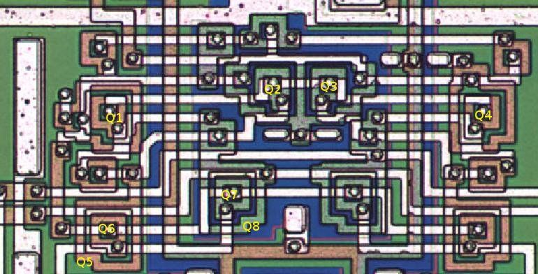
Next up is the structure just under the register array. This must have the bit line drivers.

The interface to this cell includes the four bit lines exiting at the top, four control lines traversing horizontally, and two more signal lines entering on the bottom.
At the top is yet another oddity. A largish n well. The strange thing about this is that its connection to the power rail is controlled by a transistor: that long dual gate structure in the center. There are two pairs of transistors in this well but it is also connected to all of the P channel transistors in the register file. This is weird. What I suspect is happening, but this will require more digging to verify, is that it is part of the register write process.
The bit cell is just a pair of cross connected inverters and they are happy in whatever state they are in. The usual way of changing the state is to drive a bit line using a driver that is more powerfull than the inverters. It appears here that instead the P channel FETs are disconnected from the power supply.
Yes the power is disconnected during a write. The key is to follow the polysilicon-n diffusion guard band. This completely encloses the p transistors in the SRAM cells along with Q1 and Q2. The only connection the SRAM cell p transistor sources have to power is through Q1 and Q2. So if a write cycle takes too long (you stop the clock at just the wrong time) the 31 bits that aren't being written will fade away. Unless the control circuit limits the write cycle time in a clock independant way.
With the p channel half of the inverters disconnected from power the only thing preventing the memory cell from changing state is the gate charge on the n channel FETs.

Q7-Q12 form a pair of inverters with tri-state outputs which drive the bit lines for this column. There is an inverter just below that inverts the control signal. There is another inverter tucked into the mirror image to invert the data. This is because there are two bit lines per column that carry complementary data. The difference between the two columns is that they use separate control signals and one control signal drives Q2 and the other Q1. Q3-Q6 provide a little extra high side drive capability. (I didn't bother with the mirror version of Q7-Q12.)
If you want to write data to the left column, provide data and then strobe the control line labeled "STB_A" high. Use "STB_B" for the right column. The pulse width of the strobes must be strictly limited or the gate charge on the cells that aren't being written will fade away.
Next up is a 2 to 1 mux and latch exactly like that used to drive the address output pins so I will not give a detailed description. Data enters and exits via the poly-silicon lines at the bottom.
I keep thinking that a lot of transistors could have been saved by making the register array 32 rows by 8 columns. You lose the multiplexers but perhaps the decoder would make it a push.

This is a fairly complicated circuit with 40 transistors. It has lots of signal lines traversing the cell horizontally and it gets data from the right. Even worse the cell to the right is different so I will have to examine all eight of them.
(You might have noticed the two vertical poly-silicon lines that run between the p+ and n+ diffusion regions. These are connected to Vdd. At least they appear to be given the contacts with the p+ diffusion. The October 1977 IEEE paper has a diagram where this is annotated as a "field-shield".
This section can be broken into two parts.

The inverter on the signal A is located off this image to the left while the inverter on carry in is here. (Q17, Q18). Carry in feeds in from a similar (but not identical) structure on the right.
A determines if the data coming in from the register array above is inverted or not. If A is 1 the inverted data is present on X1. Carry in does the same for output X2.
X1 is one input of a NOR gate (Q13-Q16) while Carry in is the other. The output of the NOR gate is routed out to the left.
This appears to be a ripple carry chain. Keep in mind that there should be a carry out only if there is a carry in and this bit is a one.
The circuitry for the next bit to the right uses a NAND gate where a NOR appears here and the control of the transmission gates by signal A is inverted. This makes sense if you think about it for a bit. Carry out is carry in AND b(x) but in order to do that you need to add an inverter to the NAND gate. Which requires space. (OK, there is an inverter hanging off this signal line anyway so there is no space saved. But it does make it faster.) The transmission gates on the left have a gate ring around them to isolate them from power. (Q21-24) The isolation transistors do not get a reference designator.
The ripple carry chain here is probably one of the slowest circuits on this chip. A signal has to pass through 4 NAND and 4 NOR gates and settle for the latch that must be somewhere. (So this 8 bit incrementer can do a 16 bit increment.)
If there is a ripple carry, there must also be an XOR gate (half adder) hiding somewhere. While it isn't obvious, the inverters and transmission gates at the top are an XOR gate. When CARRY IN is 0, inverted data is routed to X2 and when it is 1, X2 gets uninverted data.
Note that you can use this to decrement as well if you invert the input and output. A decrement might require two passes through in order to get the two inversions. (Carry into the lsb would be zero on the second pass.)

The next section appears to be some type of latch. When the control line is low the transmission gates of Q22-Q24 are enabled connection the data path to the drains of Q30-Q32 but that transmission gate is disabled. The result is that the data path is connected to one input of the NAND gate.
If the other input of the NAND gate is zero, it doesn't matter what the data in is, its output will be zero. But if this input is a one, the output will be the inverse of the data. Once the control line goes high, the feedback of this through the tri-state inverter (Q29-Q32) will cause the NAND gate to keep its state. At least until its other input goes low.
The result is a latch that can be cleared. (Note that the data could come from the register file or elsewhere in the data path.) The output of this latch is routed through an inverter but it is not routed down, instead it is goes to the left.
Not all eight bits in this row are the same. The upper 4 bits are as described here but the lower 4 bits are slightly different. The inverter on the output of the NAND gate for those four bits has a transmission gate attached so it is tri-state.
In any case all eight bits are attached to a bus that runs horizontally under this section.The four lower bits are routed to the output drivers for the N bit I/O outputs. The lower three are of course the N bits but the fourth appears to be an enable.

One notable feature of this section is the poly-silicon line running vertically down the center. This is the bidirectional data bus. You might notice where it switches from poly-silicon to metal for no obvious reason. But if you remember that the poly-silicon masks the diffusion layer it makes sense. The poly-silicon line creates an insulating barrier in the diffusion layer and because the C2L design depends on routing power in the diffusion layer, you must be careful to keep the diffusion well connected to power. Mostly that is done via connections to the power distribution system which appears here as the field-shield poly-silicon lines that run between the n and p diffusion areas.

The first circuit of note is another clearable latch. Q7-Q10 are another NAND gate and it is connected to a tri-state inverter made of Q13-Q16. Control is a signal line at the top and data comes from the output of a transmission gate (Q11-Q12).
This circuit is not used for every bit. Bit 5 and 0 instead use a NOR gate and invert the control signal. The difference is that when the control line is high, the NAND gate output is 1 while the NOR gate output is 0. So one is a preset and the other is a clear. The result is that it loads the value 0x21 into this latch. Which coincides nicely with what happens during an interrupt. The X register is set to 2 while P is set to 1.
This latch is organized into two 4 bit parts that drive a common 4 bit bus that is also connected to the lower 4 bits of the latch in the section above. This bus heads off in the general direction of the 4 to 16 decoders for the register file. So these appear to be the N, P, and X registers.
The transistors on the lower right get special treatment in the schematic. Although Q29-Q30 are common to the four inner transistors, they are isolated into pairs. As a result, Q29-Q30 appear twice since they really are two transistors with a common gate.
Q29-Q32 along with Q21-24 form yet another latch. Its input is tied to the output of the other latch while the output can be connected to the data bus. This could be the T register.
Because of all the transmission gates, data can take twisty paths from source to destination. For example, consider how the SEX instruction would transfer the new value of the X register from the N register. This is complicated because the X register is connected to the upper 4 bits of the data bus while N is connected to the lower 4 bits. First the output mux of the N register would be enabled so that its output is connected to the address bus shown entering here at the top right. The transmission gate consisting of Q19-Q20 is also enabled and finally the transmission gate of Q11-Q12 is enabled connecting the data to the latch.

A few things of note to start with. There is only one connection to the vertical data bus and it is an output. While all eight repetitions of this group are similiar, the one on the far right (lsb) is slightly different.

The NAND gate is part of a daisy chain. One of its pins is connected (via an inverter) to the NAND gate in the cell to the right. The inverter in the lsb has its input tied to ground. So the output of the final NAND gate will be low if and only if all the bits from the latch it is connected to are ones. Since this could be the inverted node of the latch, this is a zero detector.
What is odd is that a very similar daisy chain appears in the incrementer except that was optimized to eliminate the inverter gate delay. So this is slower than the incrementer. Perhaps it just doesn't need to be faster.
What is left is a pair of latches. One latch has a connection to the databus but it is output only. That uses two of the four control lines. The other two control lines operate the shifter. When A is high (and the other control line is low) the latch built around Q19-Q22 has its feedback loop disconnected. Transmission gate Q15-Q16 is enabled connecting the other latch to this one. So whatever is in it is transferred. TG Q9-Q10 is disabled and TG Q11-Q12 is enabled letting that latch hold its state.
When A is low the Q19-Q20 latch holds its state while the other latch is being loaded. Because the data out of the Q19-Q22 latch is fed to the right, the data moves along with each cycle. This is a right shifter.
The shifter control lines also control a shifter in the next group of transistors below. The drivers include multiple transistors in parallel and there are more p channel FETs than n channel. Electrons have higher mobility than holes of course so this equalizes the rise and fall times.
Because this is strictly a serial in - parallel out device, not only do ALU operations operate in the background of the next fetch cycle but any operation that loads the D register does so as well. It really can't work any other way.
This register doesn't appear on the RCA block diagrams but it is in the Intersil version. It is a latch that holds one input to the ALU.

At first glance this appears to be a mirror image of the D register. Except that it doesn't have the zero detect NAND gate and has both input and output connections to the internal data bus.

Home