The February 2014 issue of Nuts & Volts included an article on building a higher efficiency 13.8V power supply. The key feature being the use of MOSFETs as the series pass element instead of BJTs. I looked at the circuit and it got me thinking.
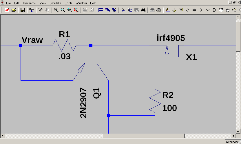
Here is an excerpt of the schematic for reference:

First some minor nits.
The one thing that stood out in the circuit and that really bugs me is the use of N channel power FETs. The usual reason to prefer N channel devices over P channel is the lower Rds(on) available. But that doesn't matter very much here with the devices operating in their linear regions and the IRF540N doesn't have outstandingly low Rds(on). (Low Rds(on) does improve dropout voltage.) Using N channel devices complicates things because of the extra gate drive voltage required. With a P channel device, that isn't a problem.
I dug out my ancient copy of the Motorola Linear/Switchmode Voltage Regulator Handbook (Link to an updated version.) and there are high efficiency LM723 circuits in there that use higher voltage supplies for the LM723. (but using BJT pass transistors.) They use an extra transformer winding to do this rather than a voltage doubler. BJTs work nearly as well as MOSFETs until you need a driver transistor for extra current gain.
So on to the variations using P channel parts. I modeled these using LTspice.

This is an image of the LTspice schematic so it isn't complete but is intended to show the changes I made.
Using a P channel MOSFET makes this a lot simpler. Gone is the voltage doubler and Zener regulator as it can run straight from the raw supply. Because the gate of the FET should go lower if the output voltage is low, the connections to the error amplifier are changed. The reference voltage goes to the inverting input while the sense voltage goes to the non-inverting input.
A pull down resistor on the gate drive is not required because I have bypassed the internal pass transistor and instead have connected directly to the output of the error amplifier at pin 13.
That is just about as simple as it gets. The one drawback of this version is that the LM723 current limiter cannot be used. If it were connected it would lower the gate voltage (increasing Vgs) when current exceeded the limit. Because that would increase the gate drive and the output voltage, it can't be used.

This is a variation on the example application in the LM723 data sheet for an external PNP pass transistor. (This one is setup to analyze load regulation.) I connected the Vz pin to ground through a diode to improve the amount of available gate drive. This helps some but requires that the current limiter be disconnected. If you need the current limiter then connect Vout to the output rail instead.
If you do that then you need higher input voltages because the gate can never go below the output voltage. Which sort of defeats the purpose of this exercise.

This is a variation on an example from the LM723 data sheet for a shunt regulator. It is a lot like the previous variation except that it uses an external transistor. It works very well but the current limiter doesn't work.
The shunt circuit has an advantage over the first two in that it has higher gate drive capability. The output of the LM723 cannot get very close to ground so this has about 6V of extra drive available. Not a huge problem as Vgs runs around -3V even at 14A out. (With excursions to -5V at the ripple minimums.)
(Power dissipation in Q1 runs a little high so you will need to check the specifications of the particular device used and adjust R5 accordingly. Or just use 1K and ignore it.)
Because the LM723 is powered from the unregulated rail in the previous circuits, ripple rejection is limited to the PSRR inherrent in the LM723. You could add some additional filtering or just power the LM723 from the regulated voltage. The major problem with this is startup.

The shunt variation is the obvious starting point because the LM723 does not need to output voltages outside of its power rails. But then the problem is startup. The gate to source resistor on the pass transistor keeps it shut off unless Q1 turns on. And Q1 can't turn on unless the LM723 sources some current. Which it can't do until the pass transistor turns on.
I tried two ways of bootstraping the regulator. The first used a weak pullup to the base of Q1. While that worked it has a serious problem in that the pullup establishes a minimum output current. The LM723 can't sink current which means that Q1 can never fully turn off. Drop below that minimum output current and the output voltage rises. Not generally considered good power supply behaviour.
The second method is shown here and is a 10V Zener diode between the regulated and unregulated rails. During startup when the output is at zero the raw rail will eventually exceed 10V and the Zener will conduct. This will bring the power for the LM723 up to the point where it can source current to Q1 and then the difference between the rails will drop below 10V and the Zener does nothing. The RC filter from the regulated rail is required to eliminate load dependence. Without the resistor the supply only starts with low loads. If the load is too high the Zener can never pull the voltage up high enough. Plus the Zener might exceed its current limit. The capacitor is mainly there to provide a low impedance supply to the LM723 but also acts as a filter.
The LM723 normally pulls so little current that the voltage drop in the resistor is around 0.1V which does not effect operation.
This works but adds more parts to what was a simple design. If you really demand low ripple (simulated at around 100uV with 4V of ripple on the raw rail) then this will get the job done. Otherwise stick to the simple variation #1.
The current limiting circuitry in the LM723 cannot be used in these designs but it can be added easily. All that is required is a sense resistor and a transistor:
When the voltage across the resistor exceeds Vbe of the PNP transistor, the transistor pulls the gate up to the source, reducing the gate drive and limiting current. This works great except in the shunt variations where it results in dueling transistors. Here it just overwhelms the limited output drive of the LM723. (The output transistor is one half of a differential pair and the maximum possible current is only twice what it normally carries.)
In the shunt variations you could put a NPN transistor on the return/ground side of the output and have it pull the base of the shunt transistor down. But this also results in dueling transistors because the LM723 is trying to drive it high. So just use a high side current limiter with a resistor (200 Ohms, 1/2 Watt) to limit current.
A note appeared in the following issue concerning over voltage protection and the author responded. The suggested circuit also appears on page 99 of the Motorola/On Semiconductor handbook. But that circuit happens to be discouraged because it could damage the SCR. (A big bold "NO!" appears next to it.) For more details, see the book.
To get better performance requires ditching the LM723.
While the reference is OK the LM329 is better. The opamp design is decades old and much better devices are available now. At that point, it isn't a LM723 based regulator anymore which brings this to an end.
Just in case someone might like to look at the models I made, here they are:
These vary from the images above because I couldn't stop fiddling with them. One of the advantages of simulation is that you can quickly make changes and see what happens. Another is that you never ever blow things up.
Besides the variations above I have included a model of circuit from the article.
One of the few issues of Popular Electronics that I still have is from June 1975 and it has an article on designing power supplies. Its criteria for capacitors is to choose one with a time constant three times the ripple period. The time constant being calculated from the capacitance and effective load resistance. In this case 13.8V/14A. Or C = 3 X 8.33ms/0.99Ohm = 25,000uF. This was an absolute minimum value with more recommended.
Section 8 of the handbook I linked earlier includes the design information from O. H. Schade mentioned in the article if you don't want to dig up the IRE publication.
The application of this method in the article does not match the example in the handbook. The equation for the ripple factor there is:
$$ r_f = \frac{V_{Ripple(pp)}} {2\sqrt{2}V_{C(DC)}}\times100\% $$ (Eq. 8.1)
In order to calculate the peak ripple voltage you first need to know the average voltage under load yet this is not mentioned in the article. It appears that rf * VM was used instead. When Equation 8.1 is used 20,000uF is shown to be too small since Vc is 15V (calculated using Figure 8-3) with 4.2V peak ripple.
Calculating the required filter capacitance is fairly easy using the fundamental equation that relates current to voltage in a capacitor:
$$ i=C \frac{dv}{dt}$$
Since the current and capacitance are constant the integration is simplified. If you draw 14A from a 20,000uF capacitor, dv/dt will be i/C = 700V/sec. Or a drop of 5.8V in 8.33ms. (The period with a 60Hz line voltage.) So 20,000uF isn't enough.
Based on the LTspice simulation the ripple voltage is about 4V for a dv/dt of 480V/s and minimum required capacitance of 14A/480V/s = 29,000uF. The actual dt is a bit lower than 8.33ms because the transformer supplies current for part of each cycle and dv will be lower as well because the capacitor is only called on to source the full 14A for part of each cycle. But this is a good first approximation.
Here is a plot of capacitor (1X20,000uF) voltage and current:
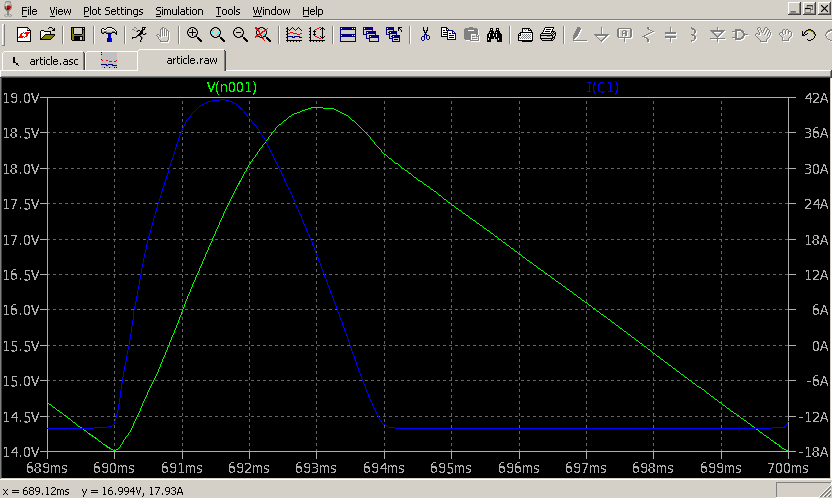
I used a vendor model of the bridge diode and transformer impedance from manufacturer specifications with a 22.2V peak supply voltage. The capacitor voltage stays just above the voltage where the regulator would drop out of regulation.. Note the very high ripple current of 20A RMS. While 20,000uF is just barely enough here, it allows zero margin for line votlage variation or capacitor aging. (The capacitor ESR in particular will get worse with age. With the high ripple currents it is going to get old fast.
By using a higher voltage transformer you can tolerate more ripple and use less capacitance. But if you use a transformer with too little output voltage in order to improve efficiency, you need really big capacitors.
The 20,000uF used (Or is it 30,000uF? The part number listed in the parts list is a 15,000uF part even if the parts list says it is 10,000uF.) is too low and should be increased. A benefit of adding two more of the 15,000uF parts is that the inadequate ripple current specification will be improved.
The heatsink calculations are completely wrong even if the chosen heatsink is acceptable.
The article starts with a temperature limit of 175°C (which is for the junction) but then focuses on the case temperature and the derating of the absolute maximum power dissipation figure with case tempertature. Completely ignoring the junction to case and case to heatsink thermal resistance. (1.15 and 0.5 °C/W respectively) If you include all of the thermal resistance values, the junction temperatures would be 238°C. (Three transistors on 0.5C/W heatsink) So its a good thing that the power dissipation used is much too high.
The power dissipation calculation starts with a constant 20V unregulated supply figure. As can be seen in the section above on capacitors, at high current it is far from constant. Going back to the simulation the RMS average of Vds is 2.6V with a 14A load. It is even lower at 20A because it drops out of regulation so I will do the calculations at the rated 14A load.
Power dissipation is 2.6V X 14A or 36.4W. If just one transistor is used, the temperature rise would be (1.15 + 0.5 + 0.5) X 36.4 = 78°C. That assumes mounting without an insulator but with heatsink grease. This is well within the capabilities of the IRF540N.
Backing up and starting over, if we desire to limit the junction to a maximum of 125C (failure rates rise quickly with temperature so you want to stay far away from the absolute maximum) at an ambient temperature of 25C, then the total thermal resistance must be no greater than 100C/36.4W or 2.7C/W. Subtracting the package and mounting thermal resistance of 1.15 + 0.5 + 0.6 means that a heatsink of 0.5C/W is required.
Adding an insulator is tricky to model. If you can find one of the 2 mil mica insulators discussed in the handbook they have a thermal resistance of 0.6°C/W. But you are more likely to find 10 mil parts that are closer to 2°C/W. If you use an insulator that has a 2°C/W rating then splitting the power dissipation over a pair of transistors looks better. The heatsink then needs to be rated at: 2.7C/W - (1.15 + 0.5 + 2.0)/2 = 0.88C/W. (Or 1.5C/W with 3.)
If you skip the insulator then the heatsink should be electrically isolated and protected to prevent shorts.
The Newark heatsink part number shown is not rated at 0.5C/W as you might expect after reading the article but 1.1C/W. More than adequate as it turns out.
The final design depends on the heatsink insulator. Skip it and a single transistor on a smaller heatsink is required. Pick a bad one and you either really do need that 0.5°C/W heatsink or a pair of pass transistors on a smaller one. Given the prices, an extra transistor is probably cheaper.
I looked at P channel devices and the IRF4905 in a TO220 case looks reasonable and as a bonus it has a better junction to case thermal resistance of 0.75°C/W.
While the heatsink rating is important, the bottleneck is the junction to heatsink connection.
This is all based on simulations which may be differrent from reality. Although the articles author provided some measurements that helped, there is still the possiblity that it diverges from reality. This is what design margins are for.
Home