Long ago, Transolve designed and sold an altimeter for model rockets that was built around the CDP1802 micro-processor. The owner of Transolve published an article describing it in Radio Electronics in October 1990. I stumbled onto that article a few years ago and have been curious about it ever since. So when one appeared for sale, I couldn't pass it up.
The article included a binary dump of the firmware in the 2K EPROM. Less than 512 bytes were used. I spent some time typing it in (The BBS mentioned in the article having long since vanished with no trace that I could find.) A pass through a disassembler let me have a look. The code appeared to have been hand assembled. Gaps in the code, dead code, etc.
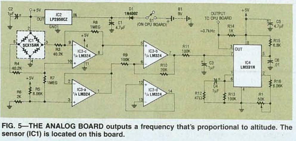
The instructions instruct you to adjust the poteniometer on the analog board before every flight. Done with the display connected so that it reads 50 feet. The pot is on the voltage to frequency converter IC and I expected that to be an offset adjustment. But consulting the data sheet showed that it was a gain adjustment. How you can get any accuracy at all with variable and unknown gain is unexplained.
The sensor used is the SCX15AN which oddly enough I found still in stock at Mouser. (But at a very high price.) The output (less than 100mV full scale) is amplified in a couple of stages using the LM324. One opamp in the LM324 (quad opamp) is used to buffer a resistive divider to provide 1V.
The output voltage from the sensor isn't exactly obvious. The data sheet specifies a full scale span of 90mV. Without making it clear that this is with a 12V excitation voltage. With 5V excitation as is used here the span is going to be 5/12 of that or 37.5mV. The article is also very pessemistic about accuracy over temperature. I couldn't find a data sheet from 1990 but the more recent ones indicate a wide temperature range.
At first glance I thought the LM324 was configured as a classic 3 opamp implementation of an instrumentation amp. A closer look showed it to be much simpler. IC3-c is configured as a differential amplifier. Ignoring the sensor output impedance its gain is 25. But the sensor is high impedance, about 4K, so the actual gain is less. (An instrumentation amp wouldn't care about the source impedance.) About 23. IC3-b provides an additional gain of 1.2. One odd thing about thiscircuit is that the polarity appears inverted. The sensors + output goes to the inverting input.
I decided to whip up a SPICE model (LTSPice actually) to verify what was going on. This verified that the output of the opamp circuit goes from around 1V at minimum pressure to near 0V at maximum pressure.
The output goes to a LM331 voltage to frequency converter. Sort of a higher tech version of the LM555. The LM331 has a current generator (voltage referenceplus external resistor) which is used to charge a capacitor. Accuracy and stability are compromised by using a tantalum capacitor instead of something a bit more stable and accurate like mylar. (Which would be larger so there is a tradeoff.) The output (ca. 3KHz) is divided by 256 before being sent to one of the EF inputs of the 1802.
The code in the 1802 is pretty simple. Increment one of the 16 bit registers, test the flag and continue till it fails. A two instruction loop or 32 clocks per loop. The article text says the clock is 2MHz while the schematic says 1MHz. The crystal was installed with its markings facing the board and somebody pookied it in place with some RTV (a good thing) so chance of reading that. Time for the o-scope.
The code checks the count to make sure it isn't exactly 1. Which would probably be some sort of glitch. Hard to imagine that since the output of the divider is going to have an exact 50% duty cycle.
A significant limitation of this system is the lack of a timer to schedule conversions. So the only timing source is the variable frequency output from the sensor. If the CPU were in a socket I would be tempted to replace it with a CDP1804 which has an integrated timer.
The data is stored into SRAM for playback later. Once on the ground, you can connect a box with a LCD display and a few switches. Do not turn the altimeter off or all of the data in SRAM (no backup power) goes away.
The display is in the form of several seven segment characters. The display controller knows nothing of this and just controls 31 outputs. The program must convert the 16 bit count into altitude, then output 31 serial data bits in the appropriate order. So I would expect to find a /MOD by 10 sort of function somewhere. Nothing. No subtract opcode to be seen.
There is a section of code that does some peculiar things to a series of bytes in memory. As in check to see if they are equal to 9 before incrementing. It appears that the method of converting the binary number into decimal is to increment a BCD value while decrementing the binary value to zero. Simple, but slow.
An unexpected bonus was that this altimeter came with a daughter board and firmware to support dual deployment. There were only two wires connecting this to the main board so I was very curious as to how it generated two outputs from a single signal line. But no schematic was in the documentation.
A little analysis of the PCB revealed an extremely simple circuit built around the CD4049 hex (six) inverter. Two simple RC filters with different time constants triggered the outputs. Hold the Q output of the 1802 high long enough and first one and then the second output will be energized.
This means that the Q output has three jobs. First is to blink an LED to provide status. Second is as the clock to send serial data to the LCD display, and last, to control the pyro outputs.
Starting with the code as published in the 1990 RE article. The code bears all the marks of hand assembly. Dead code and NOPs scattered about in gaps. Figuring out other peoples twisty code is hard enough usually but this is worse.
No subroutines of any sort are used with no SEP instructions to be found.
Disassembled source plus assorted comments and notes. A work in progress.
The ROM is labled "PARA2" and will have to wait. My EPROM programmer is old enough to predate USB by quite a bit and only has a serial interface. My workhorse system died in 2022. Or at least I got tired of it just shutting off on its own for no apparant reason. (Inspection showed bulging capacitors in the high current/low voltage CPU power supply.) Its replacement is way faster than I need but lacks many of what were standard interfaces. Like serial.